In the SC-55, the electrical connection of the resistor element is made via a VIA connection within the component: a through-hole filled with silver paste leading to the solder pad, which provides the connection to the printed circuit board (PCB).
With over-the-edge technology, by contrast, conductive surfaces extend to the edge of the component and are routed around the edge.
The difference therefore lies in the connection path.
In this article, the term PCB via connection is used to describe this VIA-based connection solution.
Learn more about:
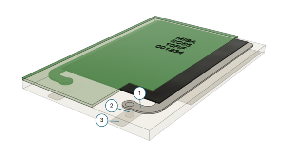
The VIA connection in the SC-55 connects the resistor element to the solder pad through a via filled with silver paste. The solder pad then provides the electrical connection to the printed circuit board (PCB).
The electrical connection consists of three elements:
1. Conductive paste: located on the top layer, it is in direct contact with the resistor paste.
2. Silver paste: fills a pre-drilled hole in the component.
3. Solder pad: connects the silver-filled via to the printed circuit board (PCB).
The via must be precisely dimensioned and properly filled. Voids should be avoided. Proper execution is essential for the electrical function of the resistor element.
With the PCB via connection, the internal resistor terminals are routed through the filled via to the solderable pads. The solder pad then provides the electrical connection to the printed circuit board (PCB).
With over-the-edge, the conductive surfaces extend to the edge of the component. The connection uses external contacts that are routed around the edge. As a result, the connection design depends more strongly on the precision and quality of the component edge.
The defined connection geometry can have a positive impact on the solder joint, electrical contact, reliability, as well as manufacturing and inspection.
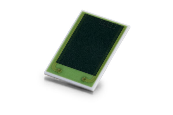
The connection is designed to provide more consistent electrical, mechanical, and thermal contact between the resistor and the printed circuit board. This can contribute to more consistent product performance.
Manufacturing and inspection: The connections are compatible with SMD processes and are particularly well suited for modern, automated series production. Clearly defined pads can facilitate optical inspection and solder-joint inspection. Fewer soldering irregularities can help reduce rework and yield losses during reflow soldering.
Have questions about the PCB via connection in the SC-55? Get in touch with us.
